
MIT launches new magnetic transistors to open a new stage for high-efficiency electronic products
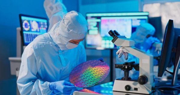
The engineering team of MIT recently announced that they have successfully developed a new magnetic transistor, and this breakthrough design is expected to revolutionize the way future electronic products operate. The device not only has a tight structure, but also has high performance and built-in memory capabilities, providing new possibilities for creating smaller, faster and energy-efficient circuits.
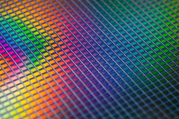
Currently, transistors are the core components of modern electronic products, but for a long time, they have mainly used silicon as their material. Although silicon can effectively control current flow, its basic physical limitations make it difficult for transistors to operate below a specific voltage, thereby limiting further reductions in energy efficiency and size. In order to break through this bottle of bottle, the scientific community has been trying to use electronic spins to design new components for many years. Electronic spins are like tiny magnets, and are expected to be a new way to control current. However, most magnetic materials in the past lacked the good electronic properties required by semiconductors, resulting in performance that never meets the standards.
This time, MIT researchers chose to replace silicon with chromium sulfur bromide to create a brand new magnetic semiconductor transistor. This two-dimensional material has both stable magnetic properties and good electronic characteristics, allowing researchers to "cleanly" switch between different magnetic conditions, greatly improving the efficiency of current control. The team is co-study author Luqiao Liu, associate professor in the Department of Electronic Engineering and Computer Science at MIT, said that a practical spintronic device is a practical combination of magnetic properties and semiconductor physics.
Luqiao Liu also stated that during the research process, the team not only found suitable materials, but also optimized the process to reduce defects, which significantly improved the equipment performance. Co-leading author Chung-Tao Chou, a graduate student in the Department of Physics, pointed out that they had tried multiple materials but failed. In the end, they found that sulfur-brominated sulfide remains stable in the air and can switch electron properties at low energy consumption, which is the key to the breakthrough.
In the production process, the team first patterned the electrode on the silicon substrate, and then accurately transferred the two-dimensional material with a thickness of only 10 nanometers. Unlike traditional use of solvents or glue water, it is moved with glue to avoid any pollution risks and ensure surface cleanliness. Benefiting from this, the performance of the new transistor far exceeds that of existing magnetic transistors. Previously, devices could only cause a few percent change in current, while the new design of the MIT team can increase the current switching range by more than 10 times, indicating potential. At present, researchers still use external magnetic fields to change the magnetic state of the material, but the energy required is far lower than that of traditional methods. More importantly, the material allows the magnetic properties to be controlled directly with current, which means that the future will allow the transistors to be operated one by one in electronic products without the need for an additional magnetic field.
In addition to the switching and amplification functions, this magnetic transistor also has the characteristics of built-in memory. The traditional memory architecture requires magnetic units to store information and then read through transistors, and the MIT design can integrate these two functions into a single component. Luqiao Liu emphasizes that the transistor can not only turn on and close, but also remember information. Due to the larger switching range, stronger signal, and the reading speed and reliability are also improved. In particular, magnets have existed for thousands of years, but this is the first time that they have been effectively integrated into electronic products, opening up a new direction for future application and research.
At the current stage, this project has received support from the US National Defense Advanced Research Planning Agency (DARPA), the US National Science Foundation (NSF), the Ministry of Energy, the International Military Research Office, the Semiconductor Research Company (SRC), and the Czech Ministry of Education. Some of the research completed by the experiments at the MIT.nano facility. The results have been published in the Journal of Physical Review Letters. In the future, researchers plan to explore how to control these transistors purely through current and develop expanded array manufacturing methods to promote practical applications.