Samsung Development SoP Advanced Packaging is used for Tesla AI6 chips, aiming at future demand
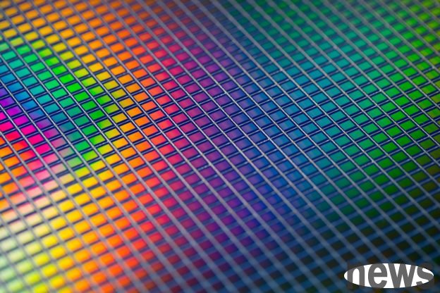
According to Korean media reports, Samsung is actively researching and developing new advanced packaging SoP (System on Panel) and promoting commercialization, in order to enter the packaging supply chain of Tesla's next generation "Dojo" super computing platform. The biggest feature of SoP is that it directly integrates multiple wafers on ultra-large rectangular panels, replacing traditional printed circuit boards (PCBs) or silicon interposer. With the ultra-micro copper redistribution line layer (RDL) connection at the bottom of the wafer, it can create modules that are much larger than the existing packaging size.
ZDNet Korea reports that the SoP panel size in Samsung's development is as large as 415×510mm, and it is a maximum module (about 210×210mm) that can accommodate a 300mm wafer round in the current semiconductor manufacturing process. Therefore, SoP can produce ultra-large wafer modules with mass sizes such as 240×240mm, and even make two at a time. The corresponding technology of TECHNOLOGY SoW (System on Wafer) is limited to the size of the wafer and cannot achieve the same size. Although SoW is similar to SoP architecture, it is packaged with a circular wafer as a substrate and has been used by Tesla, Cerebras, etc. for high-performance computing (HPC) chip production. Taiwan Power Corporation also developed an upgraded version of SoW-X in April this year, which can integrate up to 16 high-performance computing chips and 80 sets of HBM4 memory, and will be mass-produced in 2027.
Samsung is optimistic about the size advantages of panel packaging, but SoP commercialization still faces challenges, including how to connect and planarize a large number of chips at one time on super-large substrates, as well as small-scale applications in the market as super-large modules, with limited initial customer and mass production cases. However, with the explosive growth of AI computing demand, ultra-large high-performance AI chip modules are gradually rising to promote the development potential of this type of advanced packaging.
Samsung has recently signed a US$16.5 billion crystal foundry contract with Tesla to build a new chip manufacturer in the United States, producing Tesla's AI 6 chips. AI6 will be applied to Tesla's FSD (full automatic driving), robots and its own "Dojo" super computing platform. Tesla originally developed Dojo chips such as "D1" on its own, but has disbanded the relevant teams and integrated the future AI6 with the third-generation Dojo platform to form a structure to improve development efficiency. Mask said that when all R&D directions point to AI 6, Dojo 2 has reached the point of evolution, so it decided to end and make the necessary personnel adjustments, and Dojo 3 will continue in the form of integrating a large number of AI6 chips.
For high-density integration, Tesla plans Dojo 3 to adopt Intel's EMIB (Embedded Multi-die Interconnect Bridge) technology, which is a 2.5D packaging solution that connects chips through small silicon bridges embedded in substrates. If the plan is implemented, a new cross-factory supply chain led by Tesla and combined with Samsung Cylinder Foundry and Intel Packaging Test will be formed.
In the future, the promotion of high-efficiency applications such as AI servers, data centers, self-driving cars and robots will drive the demand for ultra-large chip modules and advanced packaging technology. If Samsung SoP is successfully commercialized, it is expected to occupy a place in the new high-level market.


