
Intel reveals 18A technical advantages, 2nm process for the tandem

Intel published a paper at the 2025 VLSI Technology Seminar, detailing 18A process technology and integrating all relevant information into one document. 18A is expected to significantly improve power consumption, performance and area (PPA) compared with previous generation processes, including a 30% increase in chip density, a 25% increase in performance, and a 36% reduction in power consumption under the same performance.
Compared with Intel 3, 18A has a performance increase of 25%, and a maximum power consumption decrease of 38%. The18A process is designed for various product designs from personal devices to data centers. The first product to use this process will be the Panther Lake processor, which is expected to be officially released later this year. Due to different application requirements, 18A has two logical database versions, one is high performance (HP), using 180 nanometer unit height (180CH); and high density (HD), using 160 nanometer unit height (160CH), suitable for low-power applications.
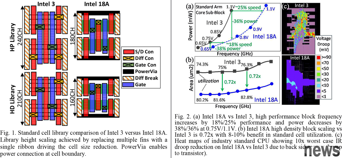
Intel pointed out that compared to Intel 3, the 18A has improved performance by 25% without increasing voltage or circuit complexity. At the same 1.1V voltage and time frequency, power consumption can be reduced by 36%; if the voltage is reduced to 0.75V, 18A can still increase operating speed by 18% and reduce power consumption by 38%. In addition, if the same design uses 18A process, the chip surface area can be reduced by about 28%.
In the SRAM part, 18A uses a high-density SRAM single transistor with a single plane of 0.021 µm², which means that the SRAM density is about 31.8 Mb/mm², which is significantly improved compared to the 0.024 µm² SRAM unit used in Intel 4. According to reports, the SRAM density of Intel 18A is comparable to that of tyrene N5 and N3E processes. However, the TEM N2 process is even more powerful, with the SRAM single shrinkage as much as about 0.0175 µm², which corresponds to a density of 38 Mb/mm².
18A with PowerVia back power supply technology to improve transistor efficiency and reduce power consumptionThe Intel 18A process is introduced into the second generation of RibbonFET gate full-circular transistor (GAA) and is paired with PowerVia back power supply network (BSPDN).
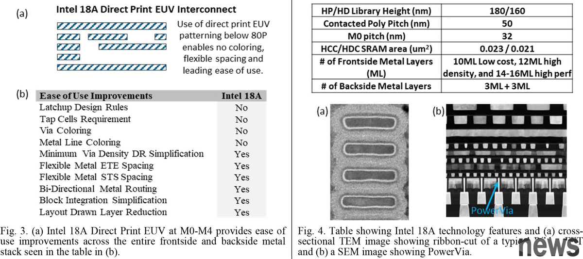
Intel 18A RibbonFET uses a four-layer nanoribbon structure and supports up to eight different logical valve voltages (VTs), including four NMOS and four PMOS, covering a range of 180 millivolts (mV).
According to a diagram in Intel's article, despite surrounding VTs, these transistors still exhibit strong electrical performance, meaning Intel successfully maintained device performance and control capabilities throughout the VT range, providing flexibility for circuit design, and balancing frequency, power consumption and power leakage in the same process.
As for Intel PowerVia back power supply technology (BSPDN), the power transmission is transferred from the top metal layer on the wafer to the back, realizing the physical separation of power and signal lines, solving problems such as rising vertical connection resistance in the rear-end process (BEOL), and also reducing signal deterioration caused by power interference, improving transistor efficiency and reducing power consumption as a whole.
In addition to BSPDN, Intel has also introduced a new generation of high-density metal-electrode-metal capacitors (MIM capacitors) to improve power stability.
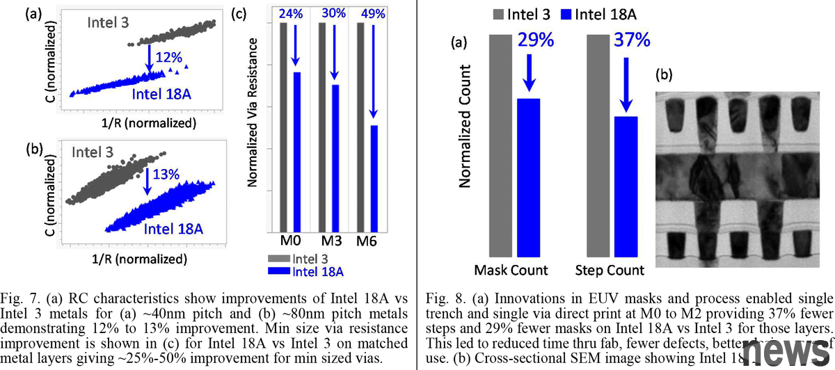
Intel reveals PowerVia's advantages, currently through JEDEC strict testsIntel also revealed the key advantages of PowerVia. Compared with Intel 3, PowerVia helps the A18 transistor density increase by 8% to 10%; the metal layer in the front section increased by about 12% in resistor-capacitor (RC) performance, and reduced through-hole (via) resistance to 49%; voltage drop (voltage drop) is reduced by 10 times; the power supply and signal lines are separated, and BSPDN can simplify chip design, making the wiring layout more efficient and flexible.
This process also uses a strict JEDEC reliability test, including 1,000-hour high-temperature aging test and extensive hot circulation tests, which proves that PowerVia can be used for designing long-lasting and strict operating conditions.
In the production part, the Intel 18A simplifies production processes and chip designs in addition to improving performance, reducing power consumption and achieving higher transistor density.
By moving the power transmission to the back of the chip, Intel does not need a traditional front power grid, and is equipped with a direct EUV exposure process to reduce the number of masks and simplify the process of the metal layer in the front section. Overall, the design process has become easier and more cost-effective.
PowerVia's back metal layer adopts a design with low resistance and high heat conductivity, which helps to effectively manage the power density brought by GAA transistors. At the same time, Intel has also improved the binding method of the carrier wafer, which can efficiently dissipate heat through the back and solve the hot challenges brought by high-performance transistors. Finally, PowerVia is compatible with advanced packaging technologies such as Foveros and EMIB, which can be seen from the Panther Lake processor using 18A process chips and Foveros 3D packaging..
Intel details 18A process technology — take on TSMC 2nm with 30% density gain and 25% faster generational performance Extended reading: No more 1.4 nano-track supercar! Samsung has changed to conservative routes, focusing on improving 2/4 nanometer yields "Intel is the only alternative option for Telco!" Analysts are optimistic about the advantages of A18 Advanced Packaging